


–
金沢大学ナノマテリアル研究所の德田規夫教授、自然科学研究科電子情報科学専攻博士後期課程/卓越大学院の小林和樹らの研究グループは、産業技術総合研究所先進パワーエレクトロニクス研究センターの牧野俊晴研究チーム長、ドイツ Diamond and Carbon Applications のクリストフ E. ネーベル CEO(本学招へい教授)との共同研究により、世界で初めて完全に平坦なダイヤモンド表面を MOS 界面(※1)に有するダイヤモンドMOSFET(※2)を作製することに成功しました。
カーボンニュートラル実現のための一つの手段として、ワイドバンドギャップ半導体を用いた高効率な電力制御が可能な次世代パワーデバイスが期待されています。その中でも、特に高い絶縁破壊電界とキャリア移動度、熱伝導率を有するダイヤモンドは、究極の半導体デバイス材料として期待されています。
德田教授らの研究グループは、これまで独自のダイヤモンド成長技術や表面・界面制御技術を開発し、世界で初めてダイヤモンド半導体を用いた反転層チャネル型 MOSFET の開発に成功しました。しかし、開発したダイヤモンド MOSFET は、MOS 界面にチャネルの散乱因子が多く存在し、動作時の高い抵抗が問題でした。そのため、その散乱因子の解明と低減に向けた研究が進められています。本研究グループは、ダイヤモンドMOS 界面の荒れがその散乱因子の原因の一つであることを突き止め、原子的に完全に平坦なダイヤモンド表面を MOS 界面に用いることでデバイスの低抵抗化を目指してきました。その結果、2022 年に開発した、完全平坦表面を持つダイヤモンド半導体層の選択的埋込成長技術を利用し、世界で初めて完全原子的平坦ダイヤモンド表面を MOS 界面に有するダイヤモンド MOSFET を作製することに成功しました。本デバイス作製技術は、ダイヤモンド MOSFET の性能向上に大きく寄与しました。
今後、本技術を発展させ、更なる性能向上により、ダイヤモンド半導体の実用化を大きく前進させることが期待できます。
研究成果は、2025 年 1 月 28 日に Elsevier の国際学術誌『Carbon』のオンライン版に先行掲載されました。
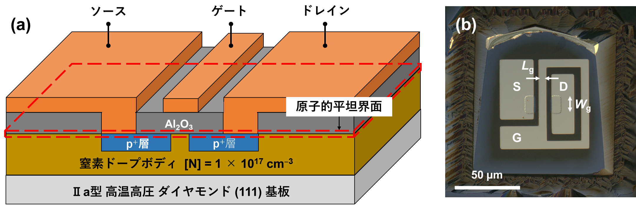 図1.今回開発した原子的平坦界面を有する反転層チャネルダイヤモンド MOSFET の(a)模式図と、(b)光学顕微鏡像。
(🄫Kobayashi et al.,Carbon, 2025)
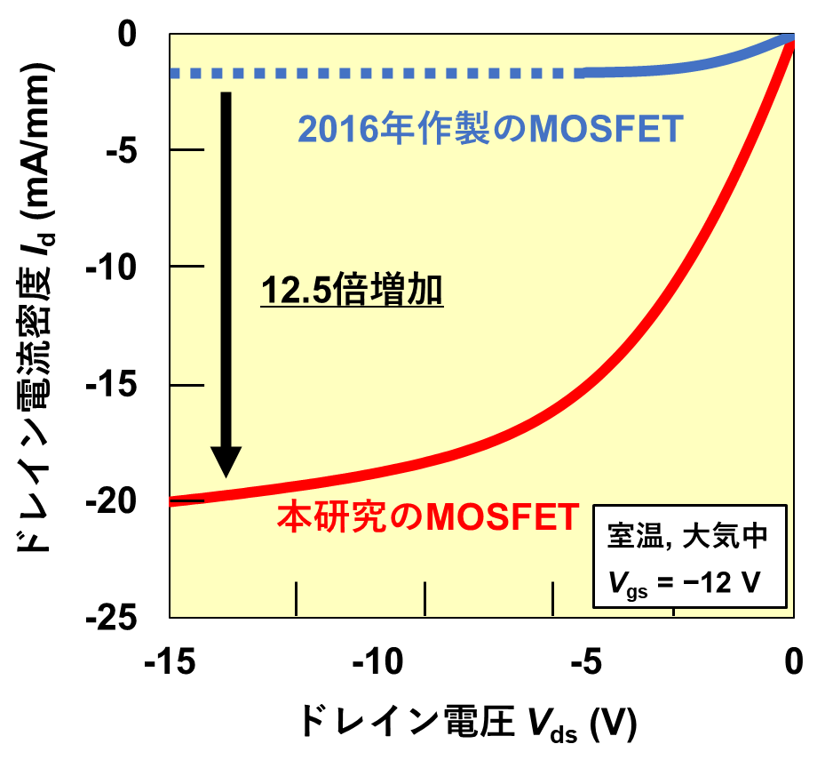
図2. 2016年に作製したMOSFETと本研究で作製したMOSFETの、ドレイン電流密度(Id)-ドレイン電圧(Vds)特性。
なお、実線は測定値であり、点線は推測値である。
【用語解説】
※1:MOS 界面
MOS は Metal Oxide Semiconductor の略称で、酸化膜と半導体の界面のことである。MOSFET のチャネルを形成する箇所となり、MOS 界面の完全性で決定される。
※2:MOSFET
MOSFET は Metal Oxide Semiconductor Field Effect Transistor の略称で、金属と酸化膜、半導体からなる界面を有する電界効果トランジスタのことである。
現在普及している半導体デバイスの多くが反転層チャネル MOSFET を基本構造としている。
ジャーナル名:Carbon
研究者情報:德田 規夫