- Home
- Highlights
- Atomically controlled diamond surfaces
Highlights
Atomically controlled diamond surfaces for next-generation high-power electronic devices
Diamond has excellent properties for high-power electronic devices. However, mechanical polishing leaves rough diamond surfaces, which diminishes the device performance. Now Norio Tokuda and colleagues at Kanazawa University, National Institute of Advanced Industrial Science and Technology (AIST) and Japan Science and Technology Agency (JST) have identified the conditions for growing flat diamond films suitable for high-performance devices.
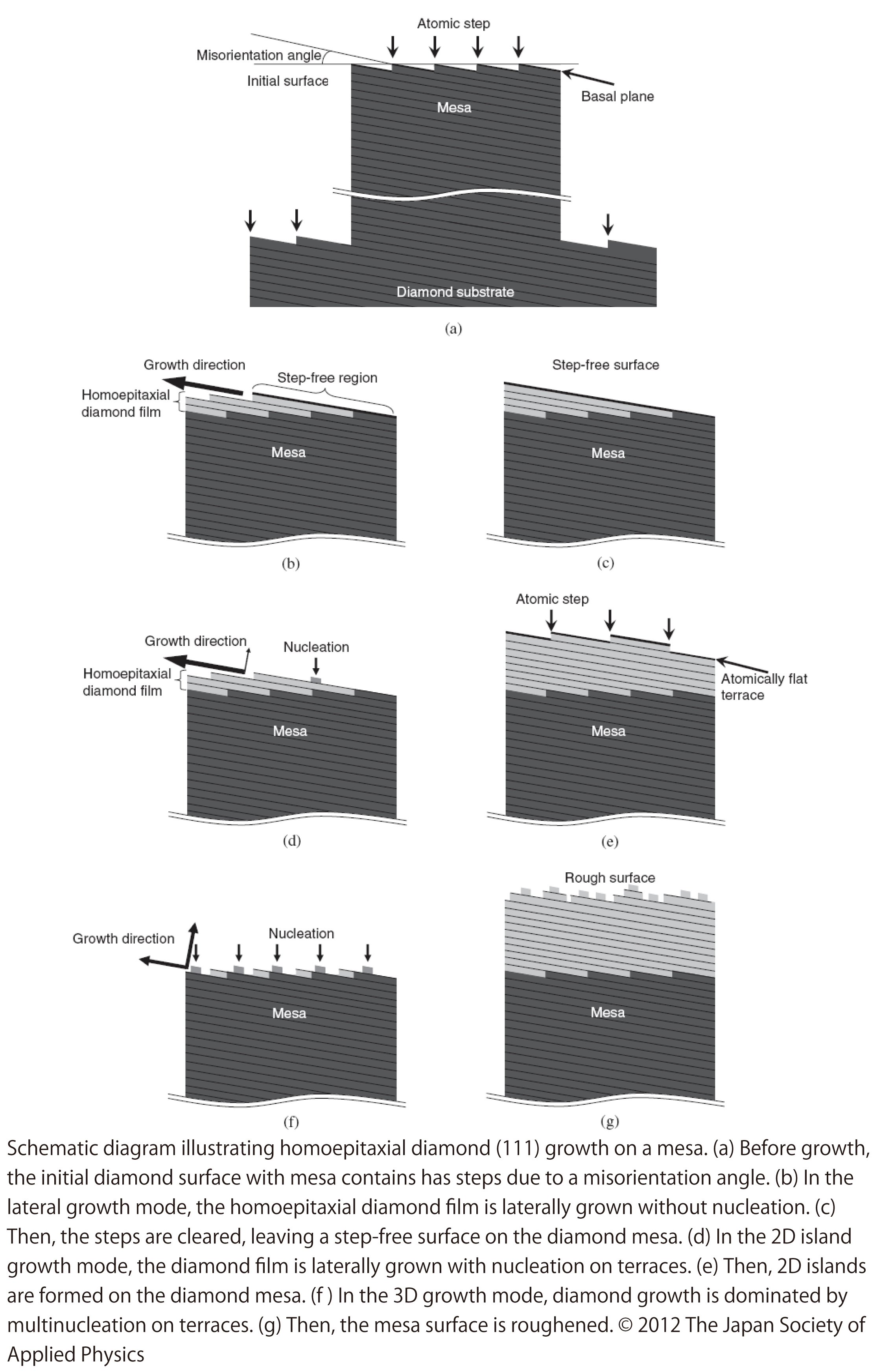
Previous work on GaN film pn diodes had suggested step-free surfaces yielded devices that perform better than atomically flat surfaces with steps. Tokuda and colleagues considered models for diamond film growth at a rough diamond surface. They identified three modes: lateral growth (only along the surface plane with no nucleation on terraces), 2D growth (mostly along the surface plane with nucleation on terraces) and 3D growth (dominated by multinucleation on terraces). Only the lateral growth mode cleared existing steps at the surface.
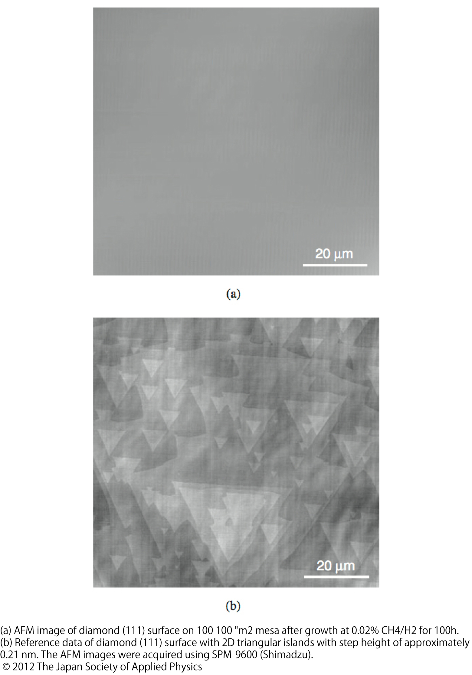
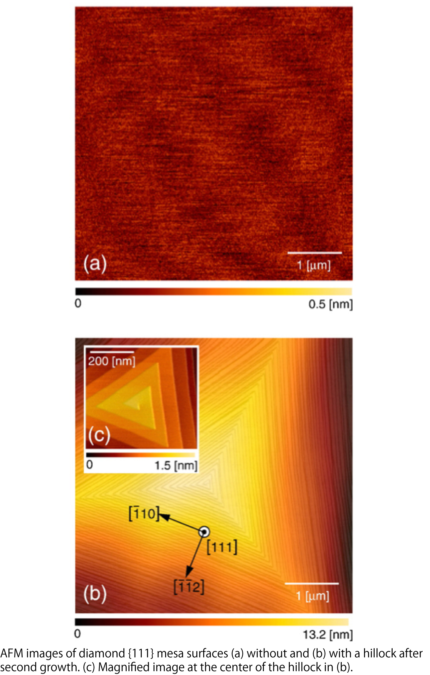
The researchers then prepared a diamond mesa pattern. The mesa surfaces had a root mean square roughness of 0.38 nm due to mechanical polishing. They deposited a diamond film on the diamond array by microwave-plasma-enhanced chemical vapour deposition of 0.005–0.5% methane (CH4) diluted in hydrogen (H2). Observations of the diamond surfaces by Nomarski optical and atomic force microscopy revealed an atomically step-free surface on 64% of the 50 × 50 μm2 mesa. Spiral hillocks attributed to screw dislocations were observed on the remainder.
Increasing the methane concentration above 0.5% resulted in roughened surfaces due to multinucleation on terraces and 3D growth. The researchers conclude, “We are sure that the lateral growth and the atomically step-free surface formation of diamond (111) films will be a key in realizing high quality for not only homoepitaxial diamond films but also heteroepitaxial films such as AlN/diamond, and, in turn, in realizing diamond devices with outstanding performance.”
Publication and Affiliation
Norio Tokuda1,2,3*, Toshiharu Makino2,3, Takao Inokuma1, and Satoshi Yamasaki2,3 Formation of Step-Free Surfaces on Diamond (111) Mesas by Homoepitaxial Lateral Growth. Japanese Journal of Applied Physics, 51, 090107, (2012). Link
1. Graduate School of Natural Science and Technology, Kanazawa University, Kanazawa 920-1192, Japan
2. Energy Technology Research Institute, National Institute of Advanced Industrial Science and Technology (AIST), Tsukuba, Ibaraki 305-8568, Japan
3. Core Research for Evolutional Science and Technology (CREST), Japan Science and Technology Corporation (JST), Kawaguchi, Saitama 332-0012, Japan
*corresponding author, e-mail address: tokuda@ec.t.kanazawa-u.ac.jp
ID: 201212A014